

dc- and ac-SECM Measurements on Si Nanowire Arrays Scanning Probes – Application Note 10
Latest updated: June 13, 2024Abstract
Si nanowire arrays are of growing interest because of their prospects in energy storage and renewable energy production device such as solar cells. In this note, dc- and ac-SECM are used to characterize the electrochemical properties of such arrays in various aqueous electrolytes. The structure revealed by the SECM maps obtained with an M470 corresponds to the structure revealed by the SEM pictures, indicating that heterogeneities in surface conductivities are related to morphological features.
Introduction
The use of SECM in energy storage applications has grown in recent years. Si nanowire arrays, of interest for their prospects in solar cells and batteries [1], were provided by GREMAN. Investigating the local electrochemical properties of such arrays can help us in understanding how to optimize their properties in operation. Local techniques can help in highlighting the electrochemical heterogeneities of these electrodes. These arrays were measured by both dc- and ac-SECM allowing their activity to be mapped, and correlated with SEM measurements.
dc-SECM vs. ac-SECM
dc-SECM is based on the measurement of Faradaic current at the Ultra Micro Electrode (UME), and therefore must be done in the presence of an electrolytic salt, and a redox active species. This species may be added to the system in the electrolyte, or it may be released from the sample. When performing dc-SECM measurements there are two distinct responses which are dependent on the sample nature. If the measured sample is conductive then the current magnitude will increase with decreasing tip-substrate distance, this is due to the regeneration of the redox species at the sample surface. When the measured sample is insulating, however, the current magnitude will decrease with decreasing tip-substrate distance, due to hindered diffusion of the species. Therefore a dc-SECM measurement provides information about both the sample topography and electrochemical activity.
It is also possible to perform SECM in ac mode. Unlike dc-SECM this technique does not require the use of a redox mediator or the addition of an electrolytic salt. This technique can be particularly beneficial when negative interactions between the sample and its environment are to be avoided. As with dc- SECM the response measured is related to the sample type. For an insulating sample as the tip-substrate gap decreases the impedance magnitude (ac current magnitude) increases (decreases). Over a conductive sample, however, the response is dependent on the measurement frequency and solution conductivity. When the measurement frequency is low or the solution conductivity high there is an increase (decrease) in impedance (ac current magnitude) with decreasing tip-sample distance. The impedance (ac current magnitude) decreases (increases) with decreasing tip-sample distance when there is a high measurement frequency or low electrolyte conductivity. As with dc-SECM the resulting measurement provides information about both the sample topography and electrochemical activity.
More information on ac-SECM can be found in the ac-SECM tutorial on the Bio-Logic website
[2] and in a dedicated application note [3].
Method
The Si nanowire array was mounted in a µTricellTM. This was filled with 5 mM [Fe(CN6)]3-/[Fe(CN6)]4- / 100 mM KCl for the dc-SECM measurement and initial ac-SECM measurement. The sample was then scanned in tap water by ac-SECM. All measurements were performed using an Ag/AgCl reference electrode, a Pt sheet counter electrode and a
25 µm Pt probe. dc measurements were performed with a probe bias of -0.25 V vs. Ag/AgCl. In both sets of ac measurements an ac magnitude of 50 mV and frequency of 10 kHz was applied to the probe, a dc bias of -0.25 V and 0.65 V vs. Ag/AgCl was applied for the measurement in 5 mM [Fe(CN6)]3-/[Fe(CN6)]4- / 100 mM KCl and tap water, respectively. The dc measurement was performed using sweep scan mode over a 2500 μm x 2500 μm area with a 16.67 μm step size. All ac measurements were performed in step scan mode using a 25 µm step size over a 2500 µm x 2500 µm area.
Results
A photograph of the measured sample, and representative SEM pictures are shown in Figure 1. The SEM image shows that the walls of the cells which appear in the banded region are sides of the nanowires, while the top of this structure is due to the bunching of the tips of the nanowires. The size of these features means SECM is well suited to investigate the conductivity of these different exposed nanowire regions.

Figure 1: (a) Representative SEM image provided by GREMAN of black banded region imaged by SECM. (b) Photograph of sample measured by SECM. One can see the black banded regions (bottom, left).


Figure 2: A typical result for the approach to the surrounding Si wafer (a) and the Si nanowires (b). In both cases current decreases with decreasing tip-sample distance.

dc-SECM
Prior to performing an area scan of the Si nanowire surface the probe was first positioned in Z. Traditionally this is achieved by performing an approach curve to the sample surface. Typical results of this measurement to the Si nanowire surface, and to the surrounding Si wafer, as labelled in Figure 1b, are shown in Figure 2. It is worth noting that the surrounding Si wafer is raised with respect to the Si nanowire layer. Both approach curves indicate an insulating surface. In these measurements if the Z position for the scan is determined from the final Z position from the approach to the Si nanowires then as the tip is rastered across the surface the Si nanowires are removed from the surface. Such measurements result in the underlying Si wafer being revealed, implying it approaches to the underlying Si wafer instead. This likely occurs because of the relatively low density of Si nanowires on the surface. To circumvent this problem the Z value was determined by approaching to the surrounding Si wafer. This was used as an initial Z position, and the tip was moved incrementally closer to the surface to achieve the highest possible signal, whilst avoiding the destruction of the Si nanowire surface.

Figure 3: dc-current map measured for Si nanowire sample in 5 mM [Fe(CN6)]3-/[Fe(CN6)]4- / 100 mM KCl at -0.25 V vs. Ag/AgCl.

With a Z position determined an area scan of the Si nanowires could be carried out. An area scan resulting from measurement of the black banded region of the nanowire surface is shown in Figure 3. Obvious areas of decreased absolute current values can be seen to run diagonally across the surface of the sample, in a manner which matches the cell structure seen in the SEM. Interestingly there is an increase in the absolute value of the current outlining the diagonal pattern and the cells within. It should be noted that the electrochemical activity mapped is likely a convolution of both topographic, and inherent electrochemical effects of the surface.
ac-SECM
As an insulating sample it is expected that regardless of the electrolyte or measurement frequency as the tip-substrate gap decreases the impedance (ac current magnitude) will increase (decrease). As with the dc-SECM measurements the final Z position of these approach curves could not be used as the Z position of the probe for measurement of the surface.
The impedance and ac current magnitude maps resulting from these measurements are shown in Figures 4 and 5. Comparing these electrolytes it is obvious the measurements of this surface in 5 mM [Fe(CN6)]3-/[Fe(CN6)]4- / 100 mM KCl results in a sharper and better defined measurement than in tap water.

Figure 4: (a) Impedance magnitude and (b) ac current magnitude maps for Si nanowire sample in 5 mM [Fe(CN6)]3-/[Fe(CN6)]4- / 100 mM KCl at -0.25 V vs.
Ag/AgCl.


Figure 5: (a) Impedance magnitude and (b) ac current magnitude maps measured for Si nanowire sample in tap water at 0.65 vs. Ag/AgCl.
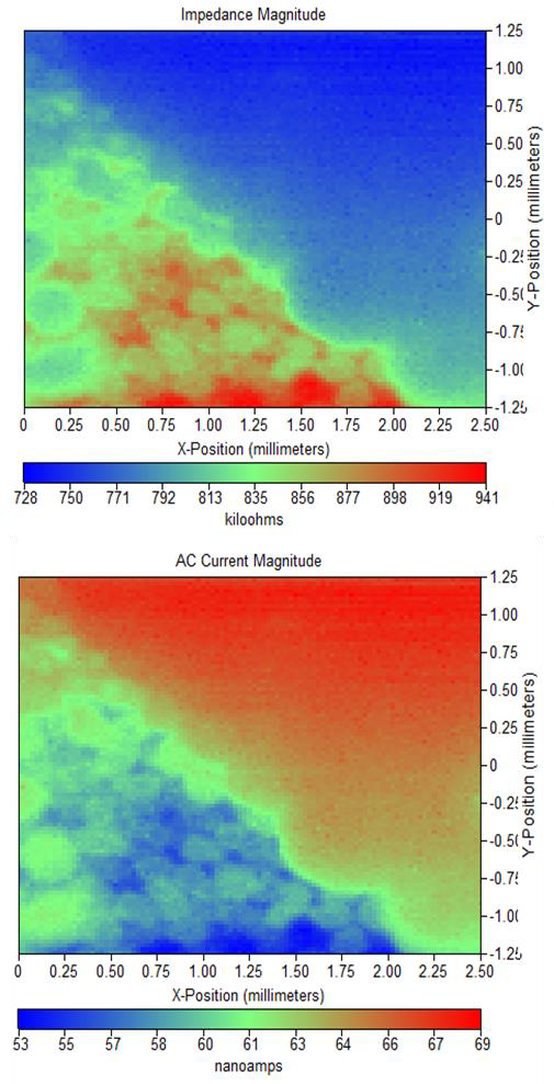
On the other hand the scans measured in tap water do show more features than those in 5 mM [Fe(CN6)]3-/[Fe(CN6)]4- / 100 mM KCl. It
is also of note that as with the dc-SECM
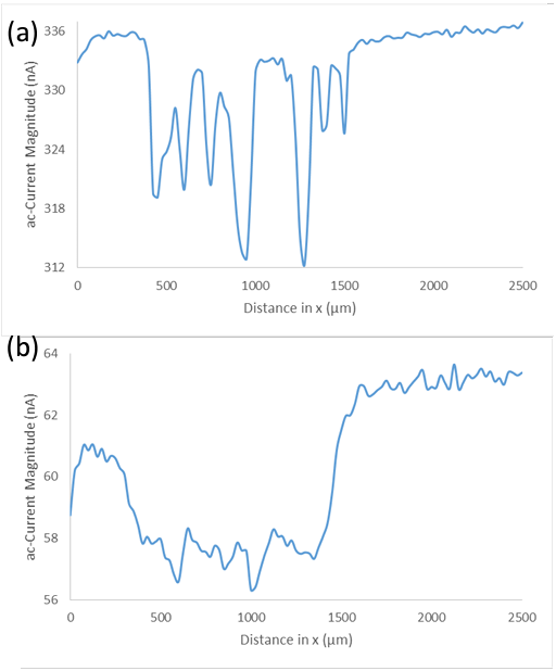
measurements, when the nanowire array is measured in tap water by ac-SECM a higher electrochemical activity is seen at the sides of the cells than at the tips, this effect is less clear in the same measurement in 5 mM [Fe(CN6)]3- /[Fe(CN6)]4- / 100 mM KCl. A cross section of these measurements at a similar location is compared in Figure 6. This comparison shows that while both systems show a similar change in activity on going over the black banded
region, there is a reduced change in activity between the voids and peaks of the black banded region in tap water.

Figure 6: (a) Cross section of ac-current magnitude of the Si nanowire sample measured in 5 mM [Fe(CN6)]3- /[Fe(CN6)]4- / 100 mM KCl at -0.25 V vs. Ag/AgCl. (b) Cross section of ac-current magnitude of the Si nanowire sample measured in tap water at 0.65 V vs. Ag/AgCl.
Conclusion
dc-SECM and ac-SECM were used to investigate the same area of a Si nanowire array. In all cases the measurement was indicative of an insulating surface. All three area scans measured show a distinct change in electrochemical activity over the banded region of the Si nanowire surface. This is likely due to a combination of topographic and surface electrochemical effects. The use of ic-SECM, the advantages of which are discussed in Application Note #6 on the Bio-Logic website [4], could allow the topographic effect to be further investigated. When ac- SECM measurements in 5 mM [Fe(CN6)]3- /[Fe(CN6)]4- / 100 mM KCl and tap water are compared, however, it is obvious that the choice of electrolyte affects the
electrochemical response measured.
Acknowledgements
The Si nanowire samples investigated in this note, and the related SEM image, were provided by Université François Rabelais de Tours, CNRS, CEA, INSA-CVL, GREMAN UMR
7347, Tours, FRANCE, http://greman.univ- tours.fr/home/.
The research leading to these results has received funding from the European Union’s Seventh Framework Programme (FP7/2007- 2013) under grant agreement n° 608575.


