

Measurement of a nano-patterned gold sample by ic-/ac-SECM Scanning Probes – Application Note 11
Latest updated: June 13, 2024Abstract
The objective of this note is to show the resolving power of M470 using a 10 µm Ultra Micro Electrode (UME) on a patterned Au electrode with features as small as 3 µm width. ac-SECM is used in intermittent contact mode with an organic electrolyte. By oversampling, i.e. scanning with steps smaller than the electrode size, it is possible to almost resolve the 3 µm features, or at least to greatly improve the contrast.
Introduction
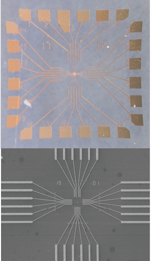
This application note aims to demonstrate the resolving power of the M470 using a 10 μm probe (Part number U-23/10). To achieve this a nano-patterned sample, Figure 1, was measured using ic-ac-SECM in 100 mM tetrabutylammonium perchlorate (TBA-ClO4) in propylene carbonate (PC). The gold on glass sample is a glass slide coated with a 25 nm titanium layer, a 60 nm aluminium oxide layer, and finally a 50-60 nm thick patterned gold layer, all patterned via e-beam process. It is this final patterned layer which is of interest in the demonstration of the resolving power. Each chip is 3.4 mm across and contains 24 off 300 μm x 300 μm pads along the edges. Connected to each pad is a 15 μm wide line which becomes a 3 μm wide line as it reaches the centre of the chip. Going to the center of the chip these 3 µm lines move closer together to become separated by 5 µm. On one side of the chip the 3 µm lines move together to make two groups of three, separated by 13 µm. The central 100 μm x 100 μm of the chip is composed of a series of isolated 20 nm wide lines.
In this application note we use oversampling, where the x/y step size is smaller than the diameter of the probe, to further resolve the sample features.

Figure 1: Top) Representative photograph and Bottom) SEM image of the nano-patterned gold on glass slide.
ic- ac-SECM
Description of ac-SECM was given in the application notes 7 and 10 [1,2]. Principles of the intermittent contact mode are given in the application note 6 [3]. For even further information on ac-SECM and ic-SECM the appropriate tutorials should be consulted on the BioLogic website [4,5].
Method
The patterned gold sample was mounted on a PTFE blank in the shallow μTriCellTM ic-SECM kit. ic-ac-SECM measurements were probe was a 10 μm diameter Pt UME, both the pseudo-reference and counter electrodes were Pt. A dc-bias of 0 V vs OCP, and an ac-bias and frequency of 100 mV and 25 kHz were applied to the probe. These values were determined from prior experiments which showed them to give noticeably different responses between insulating and conducting surfaces. Three different areas were measured:
- 1000 μm x 1000 μm with 10 μm steps
- 500 μm x 500 μm with 5 μm steps
- 250 μm x 250 μm with 2.5 μm steps.
All three measurements were positioned so focus was on the most central portion of each chip, allowing the resolution of each step size to be compared. Maps were visually processed using Gwyddion data analysis software.

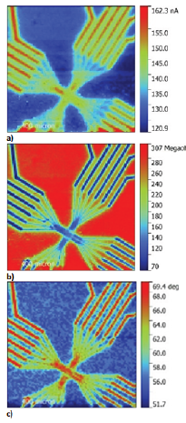
Figure 2: Measurement (1). A 1000 μm x 1000 μm area near the center of one of the patterned Au chips was measured. (a) shows the ac current magnitude, (b) the real impedance, and (c) the ac phase.
Results
Figure 2 shows the maps of the ac-current magnitude, real impedance, and ac phase resulting from measurement (1). Measurement (1) was aimed at determining the resolution of a 10 µm diameter probe when the step size is equal to the probe diameter.
All 3 images demonstrate that the parameters used in measurement (1) are adequate for resolving the 15 and 3 µm lines leading to the center of the chip.
As the 3 µm lines come together at the center of the chip, however, it is difficult to resolve each individual line. It is possible, however, to resolve the 13 µm gap between the groups of three 3 µm lines. As expected the 20 nm lines cannot be resolved, it is possible, however, to distinguish the boundary of this isolated region.
The ability of the M470 to resolve the features of the patterned gold, can be demonstrated by taking a cross section of the 15 µm lines, Figure 3.

Figure 3: A cross section of the 15 µm lines mapped during measurement (1). Dips in the impedance are due to the 15 µm lines.
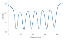
Due to the localised resolving power of the probe, the electrochemical activity decays rapidly as the probe moves from gold to glass. This decay gives rise to the shape of the cross section, and causes the full width half maximum of the troughs in the cross section corresponding to gold lines being ~25 µm, as may be expected from the probe and feature sizes. The 3 µm lines will be discussed in detail later.
Following measurement (1) the effect of oversampling on the resolution was investigated. To achieve this the step size was reduced to below the diameter of the electrode. The area of the scan was also reduced to achieve a similar number of steps per map. The results from measurements (2) and (3) are shown in Figures 4 and 5 respectively.

Figure 4: Measurement (2). A 500 μm x 500 μm area near the center of one of the patterned Au chips was measured. (a) shows the ac current magnitude, (b) the real impedance, and (c) the ac phase.
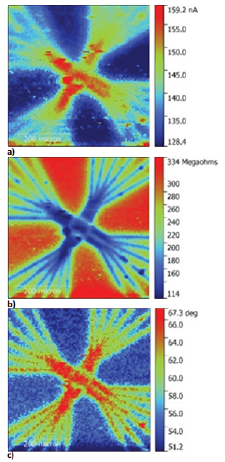

Figure 5: Measurement (3). A 250 μm x 250 μm area near the center of one of the patterned Au chips was measured. (a) shows the ac current magnitude, (b) the real impedance, and (c) the ac phase.

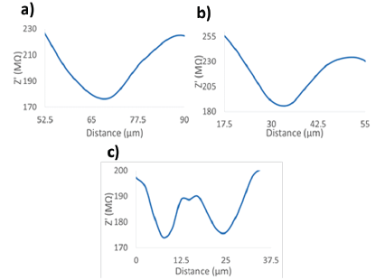
Both figures clearly show the 3 µm lines are resolved at the chosen parameters. As with measurement (1) individual lines cannot be resolved as the 3 µm lines approach the center and come down to 5 µm apart. Again while the 20 nm lines cannot be resolved the boundary of this isolated region is distinct in both scans. By measuring a cross section of the 3 µm lines for all three measurements it is possible to compare their resolution, Figure 6. To aid the comparison all three cross sections were taken after the maps were rotated to a similar orientation. The cross sections shown were also scaled to cover a distance of 37.5 µm. The width of the real impedance measured over the 3 µm line can be seen to decrease from measurement (1) to (2) to (3), as the step size begins to approach the width of the line, with the full width half maximum going from ~20.5 µm in measurement (1) to ~8 µm in measurement (3). This demonstrates that careful application of oversampling can be used to aid in improved resolution of sample features.

Figure 6: Cross sections of (a) measurement (1), (b) measurement (2), and (c) measurement (3). All were taken over the 3 µm wide line.
Conclusion
Through the use of ic-ac-SECM to measure a nano-patterned gold on glass sample the resolving power of the M470 was demonstrated with a 10 µm probe. By utilizing a step size equal to that of the probe diameter it was possible to resolve the micron scale lines of the gold patterned sample. Using oversampling it was possible to improve the resolution of these 15 and 3 µm lines. Particular improvement in the resolving of the 3 µm line was shown, which was notably smaller than the probe diameter.
Acknowledgements
The nano-patterned gold samples, and corresponding SEM images, used in this work were prepared by Dr. Jaroslaw Syzdek (BioLogic USA LLC) in the Marvel Nanolab facility at University of California, Berkeley.


